FEA also addresses its interest in the field of thin film deposition for photovoltaic applications, and the technologies adopted here have proven to be more eco-sustainable than traditional ones.
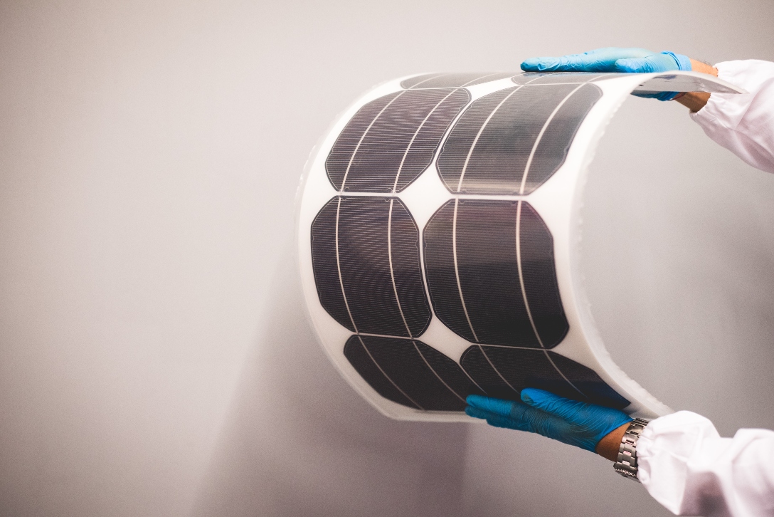
The result of this experience is a CIGS-based photovoltaic module (Copper, Indium, Gallium and Selenium) which, due to its physical and mechanical characteristics (such as reduced weight and ability to deform), is suitable for innovative terrestrial and spatial applications. This module has numerous advantages for “non-terrestrial” applications, among which: a direct prohibited band value that pairs well with the AM0 radiation spectrum, a negligible degradation when the module is subjected to both ionizing and non-ionizing radiation and finally a relative process simplicity compared to triple junction cells based on GaInP / InGaAs / Ge semiconductors.
In the Department of Electronics and new materials (aggiungi link al dipartimento two deposition technologies are adopted: the “Magnetron Sputtering” and the “Pulsed Electron Deposition” (PED). These allow to obtain thin films of good chemical (stoichiometry), structural and electro-optical quality, including a variety of different substrates and with competitive deposition times with the most advanced technologies in this sector.
PED is a technique that easily lends itself to scale-up from the level of research and development to that of large-scale production. This deposition technique allows to produce photovoltaic cells based on Cu(InGa)Se2 with an efficiency / cost ratio significantly higher than that of the techniques generally used, justifying industrial adoption. It is possible to arrive, in production, at module efficiencies above 12% and costs below 0.5 € / Wp.
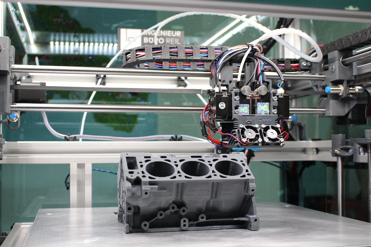
In recent activities, we have also proceeded with the idealization and construction of a machine for depositing complex semiconductors in thin films with the PED technique.
The production line developed is the result of solutions related to different optimization problems, an obligatory step to achieve the requirements necessary for the industrialization of the process.
For example, the modular feature of the line was chosen to obtain a reduction in production times and an improvement in reliability, allowing maintenance of a single module without causing the entire line to be inactive.
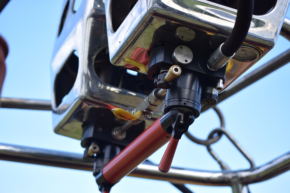
In defining the industrial production line, a new PED electronic source has also been developed which, due to its ease of use and maintenance, is suitable for both industrial and research use. The pulsed electronic beam, with a frequency of about 300 ns, penetrates about 1 μm into the impacted material producing the ablation of the latter. The cloud of dispersed particles is deposited on the desired substrate making thin films 1 nm-5 μm thick. Metals, semiconductors and insulating materials can be processed in the most diverse fields: lenses, displays, prostheses etc.